Toggle Flip Flop Timing Diagram
Toggle t flip flop. Construct timing diagrams to explain the operation of d type flip flops.
Understand timing diagrams to explain the operation of jk flip flops.

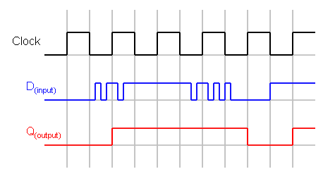
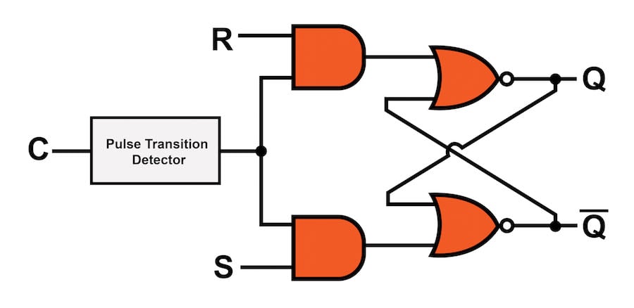
Toggle flip flop timing diagram. I have found that j k flip flop circuits are best analyzed by setting up input conditions 1s and 0s on a schematic diagram and then following all the gate output changes at the next clock pulse transition. I got some assignments for reading timing diagrams and solved it but i am not sure if it is good. Welcome i would like to ask you for explain this timing diagrams.
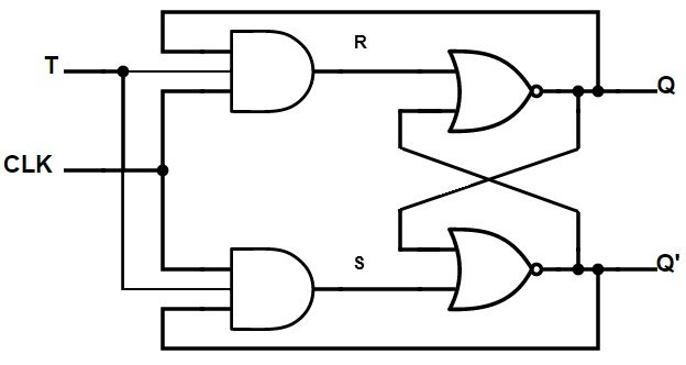
The jk flip flop augments the behavior of the sr flip flop jset kreset by interpreting the j k 1 condition as a flip or toggle command. The t toggle or trigger flip flop. This results in the jk flip flop acting more like a t type toggle flip flop when both terminals are high.
Jk flip flop timing diagram. A technique that really works well in the classroom for doing this is to project a schematic diagram on a clean whiteboard using an. Is flip flop a synchronous or an asynchronous.
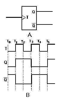
The timing diagram in figure 3 15 view b shows the toggle input and the resulting outputs. Counter design with t flip flops state diagram 001 100 010 011 111 000 110 101. Counter design with t flip flops timing diagram.
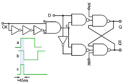
Ask question 0. A description of the jk and t flip flops along with some example timing diagrams showing how they work. Edge triggered d type flip flops.
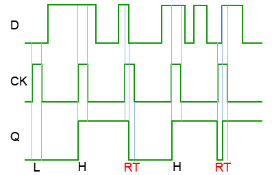
The timing diagram in figure 3 15 view b shows the toggle input and the resulting outputs. Jk flip flop timing diagram positive edge triggering. We will assume an initial condition t 0 of q being low and q being high.
February 13 2012 ece 152a digital design principles 25 counter design with t flip flops. Does the output of jk flip flop toggle continously. It is therefore.
Although developed from the basic sr flip flop becomes a very versatile flip flop with many uses. Describe alternative forms of jk flip flops. And the combination j k 1 is a command to toggle the flip flop ie change its output to the logical complement of its current value.
If logic 1 is applied to both j and k the output toggles at the trailing edge of each clock pulse just like a toggle flip flop. We will assume an initial condition t 0 of q being low and q being high. Although this circuit is an improvement on the clocked sr flip flop it still suffers from timing problems called race if the output q changes state.
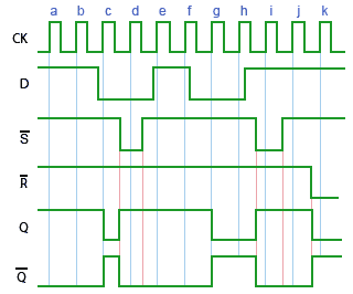
A timing diagram illustrating the action of a positive edge triggered device is shown in fig.

 T Flip Flop Block Diagram 14 16 Artatec Automobile De

 Flip Flop Basics Overview Truth Table Various Types
 Jk Master Slave Timing Diagram Free Wiring Diagram For You

 T Is For Toggle Understanding The T Flip Flop
 D And T Flip Flop
 Solved Consider The Following Flip Flop Circuitcomplete The Ti
 Flip Flops

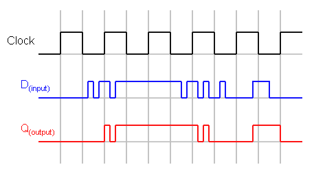

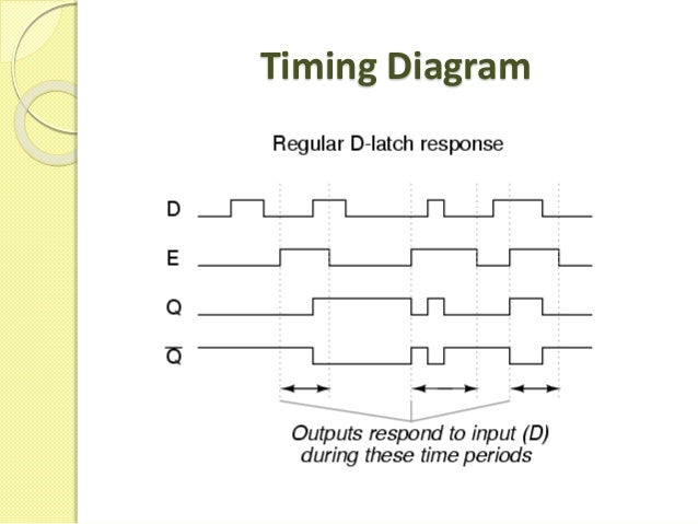
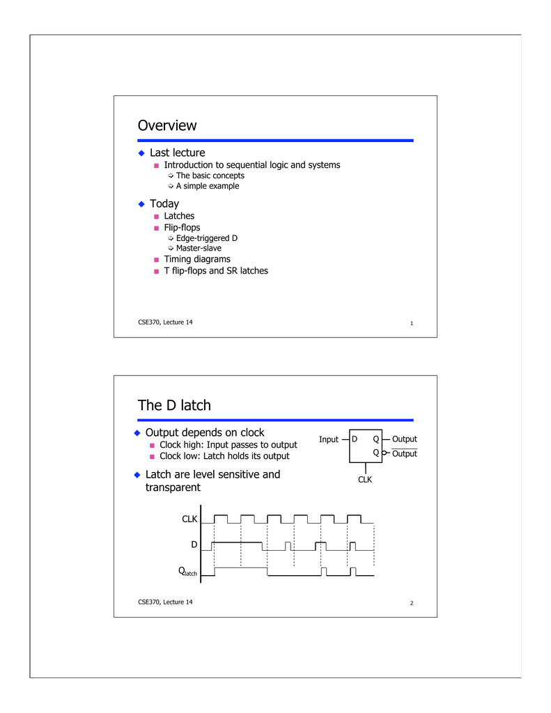
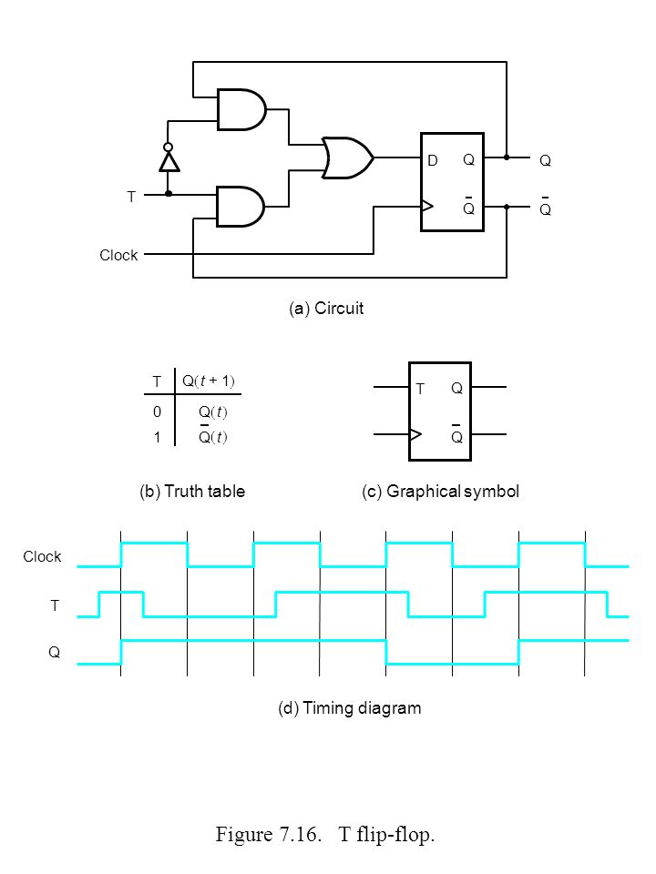 Figure 7 6 Gated Sr Latch A Circuit Q Q R S R S R Clk Q Q S Time

0 Response to "Toggle Flip Flop Timing Diagram"
Post a Comment